- 您现在的位置:买卖IC网 > Sheet目录1997 > ICS843002AKI-41LF (IDT, Integrated Device Technology Inc)IC SYNTHESIZER LVPECL 32-VFQFPN
ICS843002I-41
700MHZ, FEMTOCLOCK VCXO BASED SONET/SDH JITTER ATTENUATOR
IDT / ICS VCXO BASED SONET/SDH JITTER ATTENUATOR
11
ICS843002AKI-41 REV. B
APRIL 7, 2009
Power Supply Filtering Technique
As in any high speed analog circuitry, the power supply pins are
vulnerable to random noise. To achieve optimum jitter
performance, power supply isolation is required. The
ICS843002I-41 provides separate power supplies to isolate any
high switching noise from the outputs to the internal PLL. VCC,
VCCA, VCCO_LVPECL and VCCO_LVCMOS should be individually
connected to the power supply plane through vias, and 0.01F
bypass capacitors should be used for each pin. Figure 1 illustrates
this for a generic VCC pin and also shows that VCCA requires that
an additional 10
Ω resistor along with a 10μF bypass capacitor be
connected to the VCCA pin.
Figure 1. Power Supply Filtering
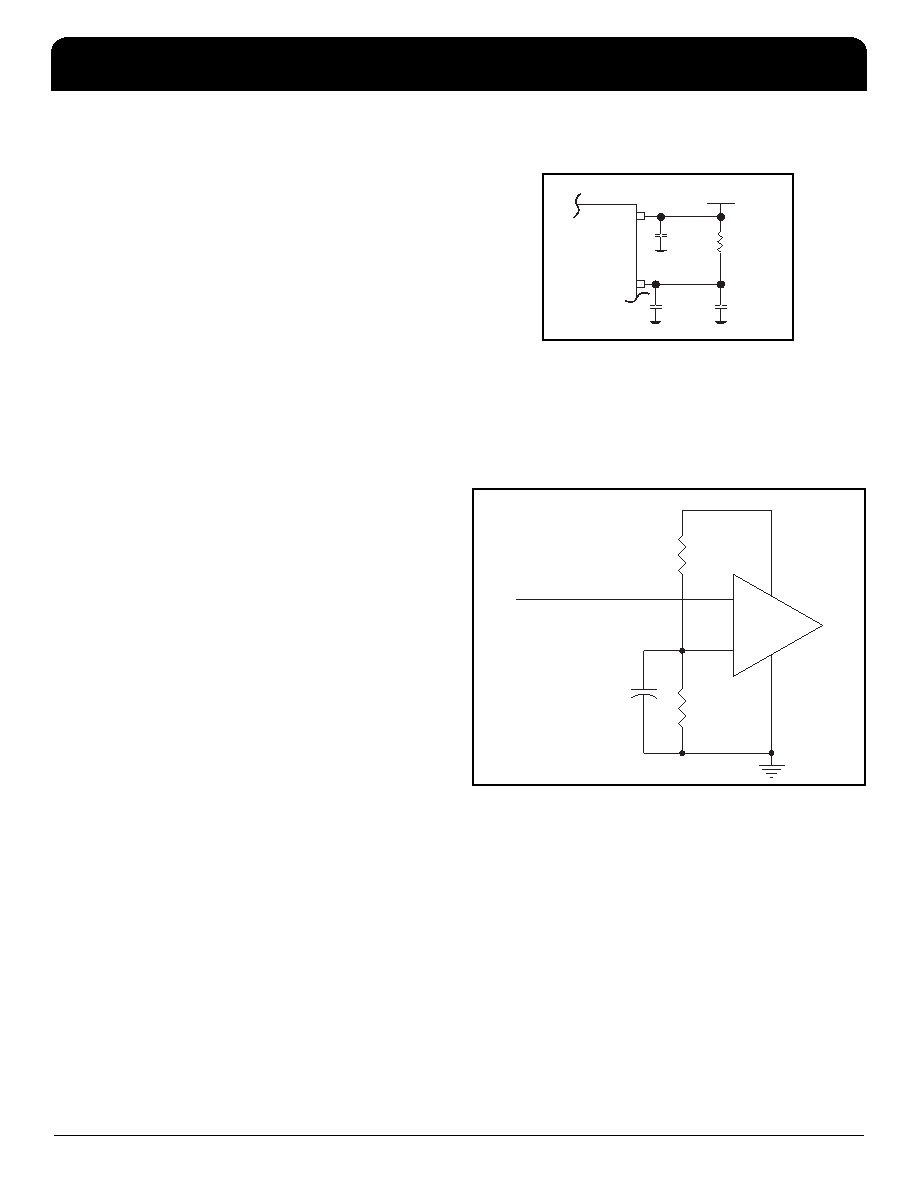
Wiring the Differential Input to Accept Single Ended Levels
Figure 2 shows how the differential input can be wired to accept
single ended levels. The reference voltage V_REF = VCC/2 is
generated by the bias resistors R1, R2 and C1. This bias circuit
should be located as close as possible to the input pin. The ratio of
R1 and R2 might need to be adjusted to position the V_REF in the
center of the input voltage swing. For example, if the input clock
swing is only 2.5V and VCC = 3.3V, V_REF should be 1.25V and
R2/R1 = 0.609.
Figure 2. Single-Ended Signal Driving Differential Input
VCC
VCCA
3.3V
10
Ω
10F
.01F
V_REF
Single Ended Clock Input
VCC
CLKx
nCLKx
R1
1K
C1
0.1u
R2
1K
发布紧急采购,3分钟左右您将得到回复。
相关PDF资料
ICS843004AG-02LF
IC SYNTHESIZER LVPECL 24-TSSOP
ICS843004AGI-04LF
IC SYNTHESIZER LVPECL 24-TSSOP
ICS843021AGLFT
IC CLK GENERATOR LVPECL 8-TSSOP
ICS843022AGLF
IC CLK GENERATOR LVPECL 8-TSSOP
ICS843023AGLF
IC CLK GENERATOR LVPECL 8-TSSOP
ICS843031AG-01LF
IC CLK GENERATOR LVPECL 8-TSSOP
ICS843081AGI-01LF
IC CLK MULTIPLIER LVPECL 8-TSSOP
ICS8430AYI-61LF
IC SYNTHESIZER LVPECL 32-LQFP
相关代理商/技术参数
ICS843002AKI-41LFT
功能描述:IC SYNTHESIZER LVPECL 32-VFQFPN RoHS:是 类别:集成电路 (IC) >> 时钟/计时 - 时钟发生器,PLL,频率合成器 系列:HiPerClockS™, FemtoClock™ 标准包装:27 系列:Precision Edge® 类型:频率合成器 PLL:是 输入:PECL,晶体 输出:PECL 电路数:1 比率 - 输入:输出:1:1 差分 - 输入:输出:无/是 频率 - 最大:800MHz 除法器/乘法器:是/无 电源电压:3.135 V ~ 5.25 V 工作温度:0°C ~ 85°C 安装类型:表面贴装 封装/外壳:28-SOIC(0.295",7.50mm 宽) 供应商设备封装:28-SOIC 包装:管件
ICS843002AKI-41T
制造商:Integrated Device Technology Inc 功能描述:IC SYNTHESIZER LVPECL 32VFQFN
ICS843002AKI-72LF
功能描述:IC SYNTHESIZER LVPECL 32-VFQFPN RoHS:是 类别:集成电路 (IC) >> 时钟/计时 - 时钟发生器,PLL,频率合成器 系列:HiPerClockS™, FemtoClock™ 标准包装:27 系列:Precision Edge® 类型:频率合成器 PLL:是 输入:PECL,晶体 输出:PECL 电路数:1 比率 - 输入:输出:1:1 差分 - 输入:输出:无/是 频率 - 最大:800MHz 除法器/乘法器:是/无 电源电压:3.135 V ~ 5.25 V 工作温度:0°C ~ 85°C 安装类型:表面贴装 封装/外壳:28-SOIC(0.295",7.50mm 宽) 供应商设备封装:28-SOIC 包装:管件
ICS843002AKI-72LFT
功能描述:IC SYNTHESIZER LVPECL 32-VFQFPN RoHS:是 类别:集成电路 (IC) >> 时钟/计时 - 时钟发生器,PLL,频率合成器 系列:HiPerClockS™, FemtoClock™ 标准包装:27 系列:Precision Edge® 类型:频率合成器 PLL:是 输入:PECL,晶体 输出:PECL 电路数:1 比率 - 输入:输出:1:1 差分 - 输入:输出:无/是 频率 - 最大:800MHz 除法器/乘法器:是/无 电源电压:3.135 V ~ 5.25 V 工作温度:0°C ~ 85°C 安装类型:表面贴装 封装/外壳:28-SOIC(0.295",7.50mm 宽) 供应商设备封装:28-SOIC 包装:管件
ICS843002ALF
制造商:ICS 制造商全称:ICS 功能描述:FEMTOCLOCKS⑩ CRYSTAL-TO-3.3V LVPECL FREQUENCY SYNTHESIZER
ICS843002BY-31LF
功能描述:IC SYNTHESIZER LVPECL 64-TQFP RoHS:是 类别:集成电路 (IC) >> 时钟/计时 - 时钟发生器,PLL,频率合成器 系列:HiPerClockS™, FemtoClock™ 标准包装:27 系列:Precision Edge® 类型:频率合成器 PLL:是 输入:PECL,晶体 输出:PECL 电路数:1 比率 - 输入:输出:1:1 差分 - 输入:输出:无/是 频率 - 最大:800MHz 除法器/乘法器:是/无 电源电压:3.135 V ~ 5.25 V 工作温度:0°C ~ 85°C 安装类型:表面贴装 封装/外壳:28-SOIC(0.295",7.50mm 宽) 供应商设备封装:28-SOIC 包装:管件
ICS843002BY-31LFT
功能描述:IC SYNTHESIZER LVPECL 64-TQFP RoHS:是 类别:集成电路 (IC) >> 时钟/计时 - 时钟发生器,PLL,频率合成器 系列:HiPerClockS™, FemtoClock™ 标准包装:27 系列:Precision Edge® 类型:频率合成器 PLL:是 输入:PECL,晶体 输出:PECL 电路数:1 比率 - 输入:输出:1:1 差分 - 输入:输出:无/是 频率 - 最大:800MHz 除法器/乘法器:是/无 电源电压:3.135 V ~ 5.25 V 工作温度:0°C ~ 85°C 安装类型:表面贴装 封装/外壳:28-SOIC(0.295",7.50mm 宽) 供应商设备封装:28-SOIC 包装:管件
ICS843002CY31
制造商:ICS 制造商全称:ICS 功能描述:700MHZ FEMTOCLOCKS? VCXO BASED FREQUENCY TRANSLATOR AND JITTER ATTENUATOR